XCZU7EV
Model
Z7-PEan
6971390278888Satisfy Network Communication, High-Speed Data Exchange and Storage Industrial Control, Deep Learning, AI Intelligence, Cloud Computing, 4K Video Transmission Processing, and Aerospace Applications
Quad Core ARM CORTEX-A53 + Dual Core ARM CORTEX-R5
Mali™-400 MP2 GPU
PS 4GB DDR4、PL4 GB DDR4
8GB eMMC FLASH、64MB QSPI FLASH

Development Software Version:Vitis 2020.1 Linux Version: petalinux 5.4.0-xilinx-v2020.1All Doucments Saved in Dropbox, after buy the board, email to get it.
Development Environment
01. Vitis Installation
02. Install virtual machine and Ubuntu system
03. Install Linux version of Vitis software on Ubuntu
04. Petalinux tool installation
05. NFS service software installation
06. QT Creator development environment
07. Linux Common Commands
Remark: Vitis 2020.1
FPGA Experiment Tutorial
01. Introduction to Ultrascale+ MPSoC
02. FPGA Board Hardware Introduction
03. Introduction to Verilog basic modules
04. PL's "Hello World" LED experiment
05. PLL Experiment Under Vivado
06. FPGA on-chip RAM read and write test experiment
07. FPGA on-chip ROM read and write test experiment
08. FPGA on-chip FIFO read and write test experiment
09. Key Experiment in Vivado
10. PWM Breathing Light Experiment
11. UART Experiment
12. RS485 Experiment
13. PL side DDR4 read and write test experiment
14. HDMI Output experiment
15. HDMI Character display experiment
16. 7-inch LCD display experiment
17. AD7606 Multi channel waveform display experiment
18. AD9238 Dual channel waveform display experiment
19. ADDA Test Experiment
20. AD9767 Double channel sine wave generation experiment
SDK Experiments
01. Experience ARM, bare metal output "Hello World"
02. PS RTC Interrupt Experiment
03. PS MIO Experiment
04. PS Side UART Read and Write Control
05. PS Side Use of I2C
06. PS Side Use of Display Port
07. PS Side SD Card Read and Write
08. PS Side Use of Ethernet (LWIP)
09. PS Side Remote Update QSPI Flash by Ethernet
10. Use of System Monitor
11. PS Side Use of EMIO
12. PL Side Use of AXI GPIO
13. PL Side Use of Ethernet
14. Custom IP experiment
15. Use of Dual Core AMP
16. Use of“Free RTOS”under ZYNQ
17. PL Read and Write PS DDR Data
18. Realize PS and PL Data Interaction through BRAM
19. DMA Loop test
20. Use of DMA-DAC Waveform Generator (AN108)
21. Use of DMA-ADC Oscilloscope (AN108)
22. Use of DMA-ADC Oscilloscope (AN9238)
23. Use of DMA-ADC Oscilloscope (AN706)
24. Use the Scatter/Gather DMA Based on ADC Module(AN108)
25. Use the Scatter/Gather DMA Based on DAC Module(AN9767)
26. AN5642 Binocular Camera Collection and Display
27. SD card read and write operation camera capture
28. Binocular camera Ethernet transmission
29. Audio Module AN831 Recording and Playback
30. Use of 7 inch LCD Module
31. 7-inch Touch Screen GUI and Touch Control
32. Ethernet Transmission-ADC Acquisition Based on AN108 Module
33. Ethernet Transmission-ADC Acquisition Based on AN9238 Module
34. Ethernet Transmission- ADC Acquisition Based onA N706 Module
35. PCle test
Linux Basic Tutorial
01. Customizing Linux with Petalinux
02. Add Boot Scripts and User Files
03. Program hello world
04. NFS service
05. Gpio Control LED
06. QT and OPENCV Cross-Compilation Environment
07. Use Vitis to Develop Linux Programs
08. SD Card Root File System
09. Vitis Accelerates Basic Platform Creation
10. From QSPI Flashstart-up Linux
11. Start the kernel from QFlash and mount the root file system from eMMC
12. NVMe SSD operation under Linux
Remark: Linux Version petalinux 5.4.0-xilinx-v2020.1
Linux Driver Tutorial
01. Character Device
02. A New Way of Writing Character Devices
03. Device Tree and of Function
04. Pinctrl and gpio Subsystem
05. Concurrent Processing
06. Gpio input
07. Timer
08. Interrupt
09. Blocking IO
10. Non-Blocking IO
11. Asynchronous IO
12. Platform
13. Platform and Device Tree
14. MISC device driver
15. Input Subsystem
16. Pwm Drive
17. I2C Driver
18. USB Driver
19. SPI Drive
20. Uart Driver
21. Block Device Driver
22. NIC driver
23. DMA Driver
24. Multi-touch screen driver
25. LCD Drive
Linux Application Development Tutorial
01. Building a Minimalist Working Environment
02. Hello World with Remote Debugging
03. OpenCV Edge Detection
04. OpenCV+Qt Face Detection
05. GStreamer's Camera Display
06. Qt+DRM+Gstreamer Camera Display
07. Qt+GPU Camera Display
08. Linux Register Operation
H.264/H.265 Codec
01. Introduction to the environment
02. Preparation for Program Operation
03. Video codec
FPGA Board
AN9767 Collection Package
AN706 Collection Package
AN9238 Collection Package
Video Package
Luxury Package
FPGA Board
●
●
●
●
●
●
Downloader
●
●
●
●
●
●
AN9767
●
●
AN706
●
●
AN9238
●
●
Binocular Camera
●
●
7-inch LCD
●
●
Supporting Modules in the Package, Click to Learn More


*Click the picture above to view the details of the core board>>

SoM Module
ACU7EVC
FPGA Chip
XCZU7EV-2FFVC1156I
Chip CPU
ARM Cortex™-A53 x4, 1.333GHz,Dual Core Cortex™-R5, 533MHz
GPU
Mali™-400 MP2
RAM
PS DDR4, 4GB, 64bit, 2400Mbps
PL DDR4, 4GB, 64bit, 2400Mbps
PS side High-Speed Connection
PCIe Gen2 x4, 2x USB3.0, SATA 3.1, DisplayPort, 4x Tri-mode Gigabit Ethernet
PS side General Connection
2x USB 2.0, 2x SD/SDIO, 2x UART, 2x CAN 2.0B, 2x I2C, 2x SPI, 4x 32b GPIO
Transceiver
12.5Gb/s x16
Chip Level
Industrial grade
Working Temperature
-40℃~85℃
Speed Grades
-2
Logic Cells
504K
Trigger
460.8K
Lookup Table
230.4K
Global Clock
8
DSP Slices
1728
MAX.DISTRIBU-TED RAM
6.2Mb
Total Block RAM
11Mb
ULTRARAM
27Mb
EMMC FLASH
8GB
QSPI FLASH
64MB
HP I/O
142
HDI/O
46
Video Codec
H.264 / H.265
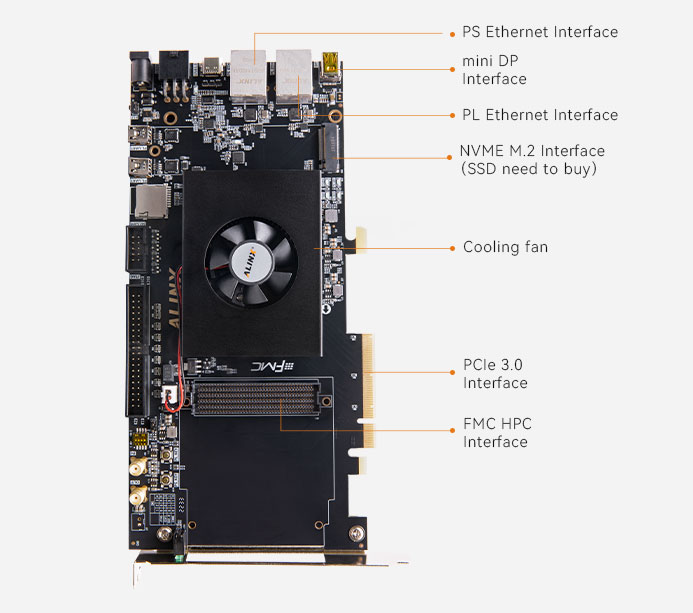
PL PCIe Gen3 x16
2
PCIe x8 Interface
Support PCI Express 3.0 Standard ( Compatible 2.0 ), Speed up to 8GBaud
M.2 Interface
Used to Connect the M.2 SSD Solid State Drive ( Need to Buy it Yourself )
DP Output Interface
1 way Mini Display Port output display interface, supports 4K@30Hz perhaps 1080P@60Hz Output ( DP to HDMI requires purchase of ALINX custom adapter )
USB3.0 Interface
1 way USB3.0 interface, USB interface type Type C supports HOST, SLAVE, OTG three modes
Gigabit Ethernet
2-way Gigabit Ethernet interface for Ethernet data exchange with computers or other network devices
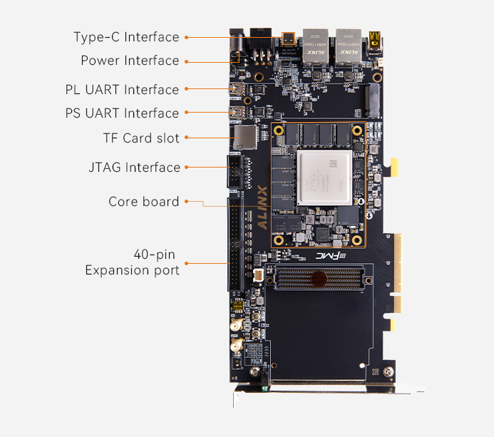
USB Uart
2 Uart to USB interface, 1 PS and 1 PL
Micro SD Slot
1 Micro SD Card Slot, Support SD Mode and SPI Mode
FMC Expansion Ports
Standard FMC HPC Expansion PortCan be Connect with Various ALINX FMC Modules (HDMI Input / Output Module, Binocular Camera Module, Hight Speed AD Module).
JTAG
10-pin 0.1-inch Standard JTAG Port for Programs Debug and Download
Temperature Sensor
Sensor Chip LM75, Used to Detect the Ambient Temperature
EEPROM
EEPROM 24LC04 with IIC Interface On-Board
Real Time Clock
RTC with a Battery Holder
LEDs
1 power indicator on the core panel, 1 power indicator on the soleplate, 1 DONE configuration indicator, 4 user indicators ( 2 mounted on the side of the panel )
KEYs
1 reset key, 2 user keys
Voltage Input
+12V DC
Current Input
Max. Current 3A
FPGA Board
1
DC Fan ( Fixed on the Board )
1
Mini USB Cable
1
USB Downloader Cable
1 Set
12V Power Adapter
1
PCIe Fence
1
TF Card
1
Card Reader
1
Size Dimension
8.74 inch x 4.2 inch
Number of Layers
16-Layer Core Board PCB, 8-Layer Carrier Board PCB Reserve independent power layer and GND layer

Intelligent identification and detection, image and video processing, security monitoring, machine vision, fire monitoring, traffic safety, smart construction site, smart hotel, smart agriculture, Internet of Things

Vehicle identification

Infrared vehicle identification

Pedestrian recognition

Indoor character recognition

Fire detection

Helmet detection

Concrete defect detection

PCB defect detection
Super Combination with Mali™-400 MP2 GPU, 64bit DDR4 RAM
4x ARM Cortex-A53, 1.333GHz; Dual core Cortex™-R5, 533MHz; PS 4GB DDR4, 64bit, Data rate 2400Mbps; PL 4GB DDR, 64bit, Data rate 2400Mbps

Intelligent Recognition, Image and Video Processing Security Monitoring, Machine Vision

The core board plus expansion board mode is adopted to facilitate the secondary development and utilization of the core board
Rich peripheral interfaces: 1 channel FM HPC, 1-way M2 SSD interfaces, 1 mini DP interface, one USB3.0 interface, one 40 pin expansion interface, two gigabit Ethernet interfaces, two UART interfaces, one PCIE3.0 X 8 golden finger, one TF card interface
It is a "professional" ZYNQ development platform to meet users,requirements for high-speed data exchange, data storage, video transmission and processing, deep learning, artificial intelligence and industrial control
Multimedia, automotive ADAS, monitoring and other embedded visual applications

Capable of simultaneously encoding and decoding 4K x 2K ( 60fps ) video
Intelligent identification, medical security, on-board digital, industrial control, smart grid

The MIP Camera Module AN5641 for Video Capture and Displays it on the Monitor through the Mini DP Interface
The ZYNQ development board runs the Linux operating system, and the video data is displayed using QT to achieve binocular synchronous display.
AN9767/AN706 Module On-Board Demo

*The Signal Source Output Signal is Connected to the AN9767 Module, and the Waveform Signal is Displayed through the Oscilloscope
*The Signal Source Output Signal is Connected to the AN706 Module,Run the System to Draw the Waveform Data, and is Displayed to the Monitor through the HDMI Interface of the FPGA Development Board
The warranty period of all products sold is 12 months, of which FPGA chips and LCD screens are wearing parts and are not covered by the warranty. All accessories and gifts are not covered under warranty.
Alinx Electronic Limited 沪ICP备13046728号