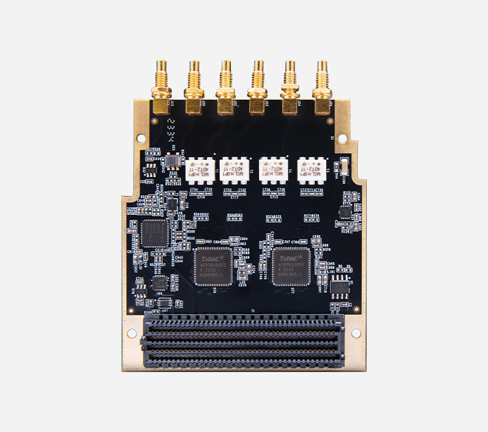
AD9781
Model
FL9781Temperature class
-40℃~85℃Price
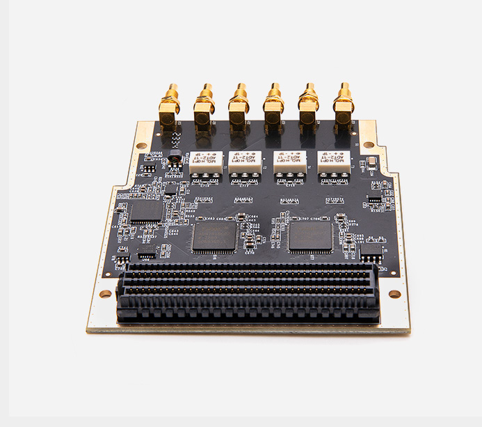
$ 1000Channel high-speed DA module, each DA has 14 bits and a 500MSPS conversion rate of digital to analog signals.

Chip model
AD9781
Number of DA output channels
4-way, 14bit, 500MS/s update rate
Output Impedance
50 Ohm
Full range output current
8.66mA~31.66mA(default 20mA)
Output amplitude range
-350mV~+350mV
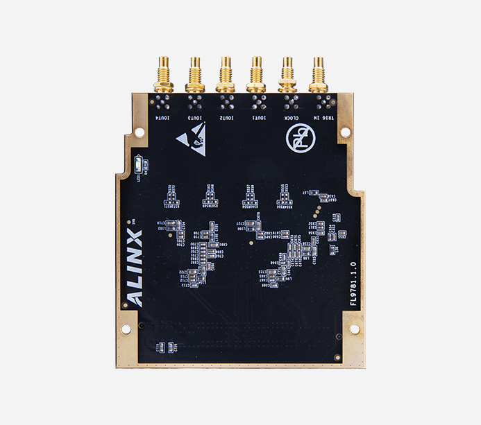
Analog signal output interface
SSMC interface
Output coupling method
AC Coupling
External Clock Input
1
External trigger/synchronization signal
1 input, 3.3V LVCMOS or LVTTL
FMC interface
Supports LPC or HPC
Digital interface level standard
LVDS level 1.8V or 2.5V
configuration interface
SPI interface
operation temperature
-40℃~85℃
consumption
Less than 6W


Hardware connection test of FL9781 module and FPGA development board

Hardware connection diagram between Z19 development board and FL9781

DA output positive selection waveform
Many development boards from Alinx have FMC LPC interfaces or HPC interfaces. All development boards with FMC interfaces support the FL9781 module.The following development boards already provide routines for the FL9781 module.
number
Development board model
FMC connector
1
AX7325/AX7325B
J7
2
AX7350
J15
3
AX7450
J7
4
AXKU040
FMC2(J6)
5
AXKU041
FMC2(J2)
6
AXKU042
FMC2(J13)
7
AXU4EVB-P
J41
8
AXU5EVB-P
J41
9
AXU9EGB
J7
10
AXU15EGB
J7
11
Z7-P
J13
12
Z19
FMC2(J33)
13
Z19-P
FMC2(J19)
The warranty period of all products sold is 12 months, of which FPGA chips and LCD screens are wearing parts and are not covered by the warranty. All accessories and gifts are not covered under warranty.
Alinx Electronic Limited 沪ICP备13046728号