ZU47DR
Model
AXRF47Price
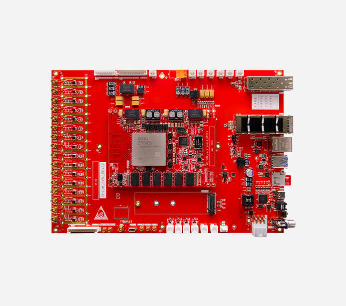
$ 13182Adopting Zynq UltraScale+RFSoC Gen3 series ZU47DR FPGA chip, integrating RF direct sampling data converter, FPGA logic, complete ARM processor subsystem, and high-speed transceiver.
Supports 8-way 14bit RF-ADC with a maximum sampling rate of 5GSPS, and 8-way 14bit RF-DAC with a maximum sampling rate of 9.85GSPS. The RF input and output frequency response fully supports the frequency band below 6GHz.
Provide a comprehensive RF signal chain, maximize input/output channel density, high bandwidth, heterogeneous processing capabilities, and low power consumption.
Meet the needs of large-scale MIMO radio, 5G baseband, fixed wireless access, cable TV access, testing and measurement, satellite communication, phased array radar/digital array radar, and other high-performance RF applications.

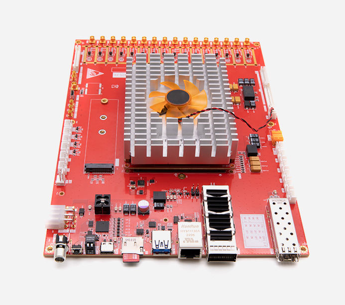
PS DDR4
PL DDR4
QSPI FLASH
8 GTY
8 14bit ADC
8 14bit DAC


*Click on the image above to view the details of the core board>>

Core board
ACRF47
FPGA model
XCZU47DR-2FFVE1156I
kernel CPU
Quad-core ARM Cortex-A53, MPCore
Dual-core ARM Cortex-R5F, MPCore
Memory
PS DDR4,4GB,64bit,2400Mbps
PL DDR4,2GB,32bit,2400Mbps
14 bit 5.0GSPS RF-ADC
8
14 bit 9.85GSPS RF-DAC
8
Decimation/ interpolation
1x, 2x, 3x, 4x, 5x, 6x, 8x, 10x, 12x, 16x, 20x, 24x, 40x
GTY / GTR
PL GTY 8 ,PS GTR 4
System Logic Cell
930K
CLB LUTs
425K
Max.Dist.RAM
13.0Mb
Total Block RAM
38.0Mb
UltraRAM
22.5Mb
DSP Slices
4272
PCIe Gen4 x8
1
DDR4
PS 4 pieces 1GB DDR4, tota 4GB, 64bit data rate 2400Mbps
PL 2 pieces 1GB DDR4, total 2GB, 32bit data rate 2400Mbps
QSPI Flash
Two 1Gb QSPI FLash chips in total, which can be used for storing FPGA user data
M. 2 interfaces
1 standard NVME M.2 interface, connected to M.2 SSD solid-state drive (requires user purchase)
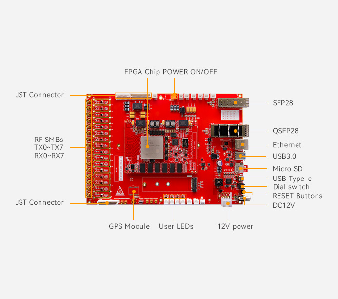
optical interface
1 QSF28 fiber optic interface and 1 SFP28 fiber optic interface
USB 3.0 interface
1 USB 3.0 interface, used to connect external USB peripherals
Gigabit Ethernet interface
1 Gigabit Ethernet interface for Ethernet data exchange with computers or other network devices
JTAG&UART interface
Type-C standard JTAG&UART interface for downloading and debugging FPGA programs
EEPROM
EEPROM AT24CM01 with 1 IIC interface
SD card slot
1-way Micro SD card holder, supporting SD mode and SPI mode
RTC real-time clock
1 built-in RTC real-time clock
LED light
4 user LED lights
key
1 reset button
Expand IO
2-way x8 PL end expansion IO, 1-way x10 PS end expansion IO
INPUT VOLTAGE
+12V voltage input
Zynq UltraScale+RFSoC heterogeneous computing architecture, including a complete ARM processing subsystem, FPGA architecture, and complete modular programmability in the RF signal chain

Main features:
1. Integrated Device of ZU47DR RF System on Chip (RFSoC)
2. Equipped with built-in digital up and down conversion and interpolation extraction functions
3. Supports 8-way 14bit transmission and 8-way 14bit reception
4. Supports 1MHz~6GHz frequency points
5. Supports interpolation/extraction coefficients of 1x~40x
EVM emission: Under typical frequency bands, EVM is better than 1%

Flatness: Output flatness at 1GHz bandwidth

phase noise


FPGA development board
1
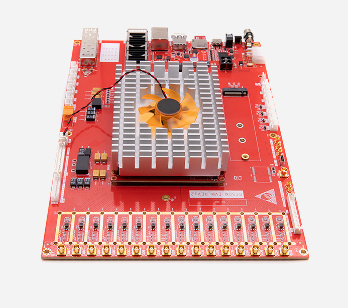
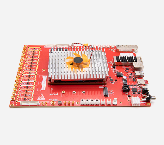
Cooling fan
1
USB to Type-C cable
1
12V power supply
1
TF card
1
1
Size
Core board 115mm x 85mm, expansion board 254mm x 180.34mm
Stacking quantity
Core board with 14 layers of PCB design, expansion board with 12 layers of PCB design, reserved for independent power layer and GND layer

Dimensional diagram of core board structure

Dimensional diagram of expansion board structure

With Zynq™ RFSoC, wireless infrastructure manufacturers can achieve previously unattainable footprint and power reduction, critical to Massive MIMO deployment.
Zynq UltraScale+™ RFSoC enables cable access multi-service operators (MSOs) to move PHY layer processing closer to home with remote PHY nodes, increasing network capacity.


As a single-chip TRX solution for scalable, multi-function, phased array radar, the Zynq UltraScale+ RFSoC enables low latency transmit and receive for optimal response time in early warning scenarios.
Designers can build high-speed multi-function instruments for signal generation and signal analysis by using direct RF-sampling, highly flexible, reconfigurable logic, and software programmability in Zynq UltraScale+ RFSoC.


Designers can build high-speed multi-function instruments for signal generation and signal analysis by using direct RF-sampling, highly flexible, reconfigurable logic, and software programmability in Zynq UltraScale+ RFSoC.
The warranty period of all products sold is 12 months, of which FPGA chips and LCD screens are wearing parts and are not covered by the warranty. All accessories and gifts are not covered under warranty.
Alinx Electronic Limited 沪ICP备13046728号