XCKU3P
Model
AXKU3Price
$ 792
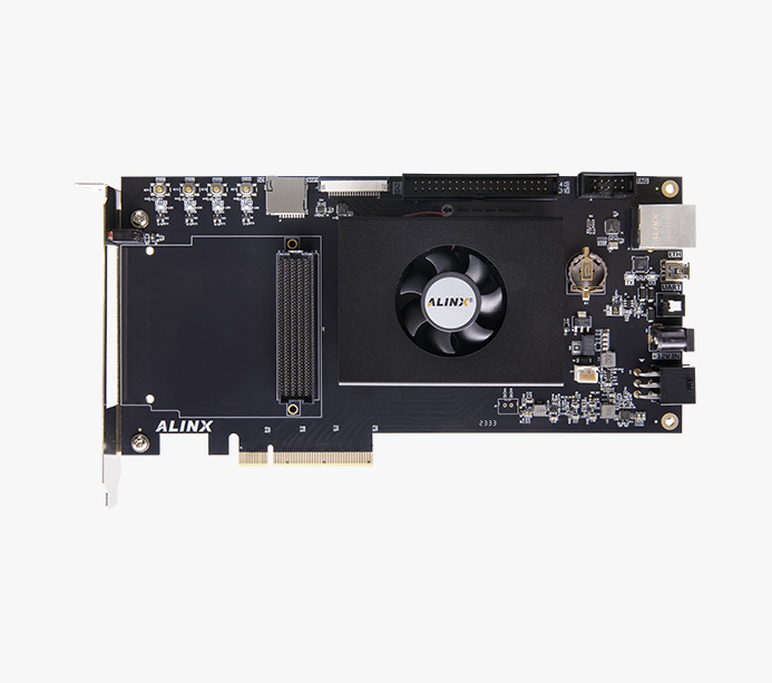
The expansion board integrates interfaces such as PCIe 3.0 x8, FMC HPC, MIPI Lanex4 camera, and Gigabit Ethernet. The core board uses 16nm process Kinex UltraScale+devices, which significantly reduces power consumption by 60% compared to the 7-series FPGA; The GTY 28Gb/s x16 transceiver and 100G Ethernet (XCKU5P) provide a cost-effective solution for applications that require high-end functionality. It is an ideal choice for applications such as wireless MIMO technology, Nx100G wired networking, and data center networking and storage acceleration, video image processing, semiconductors, industrial control, machine vision, Internet of Things, and medical imaging
356K
325K
163K
28Gb/s
Connecting various FMC cards
2GB DDR4 32bit,64MB QSPI FLASH


*Understand the core board, click to view details >>

Core Board Chip
ACKU3
ACKU5
FPGA Chip
XCKU3P-2FFVB676I
XCKU5P-2FFVB676I
Chip Level
Speed Grades -2,Industrial Grade, -40°C~85°C
Speed Grades -2,Industrial Grade, -40°C~85°C
DDR4
2GB DDR4, 32bit
2GB DDR4,32bit
QSPI FLASH
64MB
64MB
System Logic Cells
356K
475K
CLB Flip-Flops
325K
434K
CLB LUTs
163K
217K
Max. Distributed RAM
4.7Mb
6.1Mb
Total Block RAM
12.7Mb
16.9Mb
UltraRAM
13.5Mb
18.0Mb
Clock Mgmt Tiles
4
4
DSP Slices
1,368
1,824
GTY Transceivers
GTY 28Gb/s x16
GTY 28Gb/s x16
PCI Express
PCIe Gen3 x16
PCIe Gen3 x16
100G Ethernet
-
1
HD IOs
72
72
HP IOs
96
96
LVDS
45
45
DDR4
Two 1GB DDR4 storage chips with a data rate of up to 2666Mbps
QSPI FLASH
Two 32MB QSPI FLASH chips, storing FPGA configuration Bin files and other user data files
Clock Configuration
Two 200MHz differential crystal oscillators are provided on the board, which can provide reference clocks for DDR4 controllers and FPGA logic
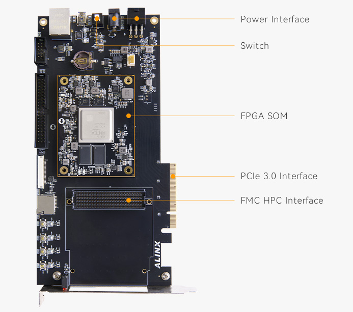
PCI Express
PCI Express 3.0 x8 interface, single channel communication rate up to 8GBaud
FMC HPC Interface
1 channel FMC HPC interface, external connection of various FMC cards (HDMI, AD, fiber optic, SDI, binocular camera, etc.)
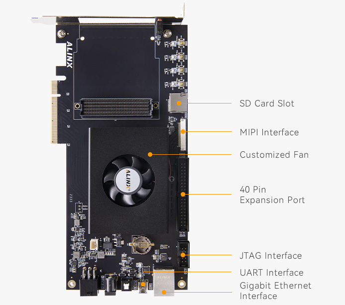
MIPI Input Interface
One MIPI Lanex4 input interface, with a speed of up to 2.5Gb/s, connected to the AN5010 MIPI camera module
Gigabit Ethernet Interface
One gigabit Ethernet interface, providing network communication services for users, with a network transmission rate of 10/100/1000 Mbps; Full duplex and adaptive
Uart Interface
1 Uart USB interface for communication with computers, facilitating user debugging
SD Card Slot
1 Micro SD card holder for storing operating system images and file systems
40 pin Expansion Port
1 40 pin 2.54mm spacing expansion port with various external modules (camera, LCD screen, high-speed AD block, etc.)
JTAG Interface
1 10 pin 2.54mm standard JTAG interface for users to debug and download the FPGA system through a downloader
RTC
On board RTC real-time clock, equipped with a battery holder (the battery needs to be purchased by oneself, model CR1220)
LED
1 power indicator light, 1 DONE configuration indicator light, and user indicator light on the core board;There is one power indicator light, four user indicators, and two serial port indicators on the backplane
Voltage Input
+12V, powered by connecting the backplane
Current Input
Max. Current 3A
FPGA Board
1
DC Fan ( Fixed on the Board )
1
Mini USB Cable
1
Platform Cable USB
1 set
12V Power Adapter
1
1
Size Dimension
8.465inch x 4.370inch
Number of PCB
Core board 14 PCB board design, extension panel 10 PCB board design, reserve separate power layer and GND layer

Dimensional Drawing of Core Board Structure

Structure dimension diagram of expansion board
8 high-speed transceiver connected to FMC HPC dedicated high-speed pins
Can connect HDMI input/output, high-speed AD, SDI input/output, fiber optic, binocular camera, Cameralink, GMSL camera and other FMC cards, freely expandable to meet high-speed transmission, suitable for development in various fields

Network Communication

Data Center Networking and Storage Acceleration

Medical Imaging

Industrial Automation

Video Imaging

IOT

ATE

Machine Vision
The warranty period of all products sold is 12 months, of which FPGA chips and LCD screens are wearing parts and are not covered by the warranty. All accessories and gifts are not covered under warranty.
Alinx Electronic Limited 沪ICP备13046728号